
The difference between the manufacturing process of DBC and AMB ceramic board carrier
Release time:
2023-03-28 15:57
Source:
summary:
In recent years, with the rapid development of power semiconductors, the third-generation semiconductor silicon carbide chips have the characteristics of band gap and high thermal conductivity. As a ceramic substrate chip carrier is used to carry the chip and connect to the water cooling system (soldering or sintering) in the end customer application to achieve the high heat dissipation, reliability and insulation performance required by the chip.

Ceramic Substrate DBC and AMB Copper Substrate Technical Process Introduction
这些年来,随着功率半导体的快速发展,在第三代半导体碳化硅芯片具有禁带宽度带、热导率高等特点。作为陶瓷基板芯片载体被应用于承载芯片并在终端客户应用中连接到水冷系统(焊接或烧结),以达到芯片所需的高散热、可靠性和绝缘性能。
At present, new power semiconductor modules based on ceramic copper substrates have been put into mass production in major semiconductor companies such as ST, Infineon and ON. The industry's demand and quality requirements for ceramic copper substrates are getting higher and higher, so engineers in the semiconductor industry urgently need to understand the manufacturing process and application risks of ceramic copper substrates. This article introduces two mainstream ceramic copper substrate processing methods on the market:
Introduction of 1. DBC direct bonding copper and AMB active metal brazing process
1, Direct bonding copper
DBC is a composite substrate that combines copper directly with AI2O3 and AIN ceramic surfaces by hot melt bonding at high temperatures. On the copper-clad surface, corresponding patterns can be etched according to circuit design or product structure. It has been widely used in the packaging of intelligent power modules and electric vehicle power modules.
2. Active metal brazing
AMB technology is a further development of DBC technology, is the use of active metal elements in the solder (such as Ti/Ag/Zr/Cu) to achieve the combination of ceramic and metal, ceramic formation can be wetted by liquid solder reaction layer.
The bonding in the AMB ceramic substrate is achieved by the chemical reaction of the ceramic and the active metal brazing filler metal at temperature. Compared with the traditional AI2O3 ceramic substrate, the Si3N4 ceramic used in AMB has a higher thermal conductivity (>90W/mK 25°C), which is closer to the thermal expansion coefficient of silicon (2.6x10 -6 /K). Therefore, the AMB substrate has high adhesive strength and reliability. Combined with the silver sintering process and high-power silicon carbide chips, the AMB copper layer with active metal coating can achieve high power, better heat dissipation and high reliability of the packaging module (can withstand 3000 thermal shocks), has been widely used in electric vehicles, electric locomotives and high-speed trains.
Main technical process flow of 2.
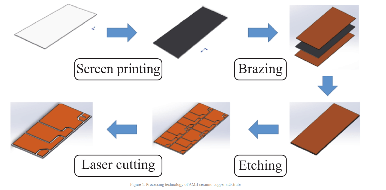
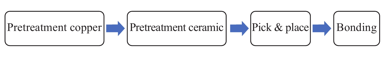
The overall process of the ceramic copper substrate is as follows: first: surface treatment of the supplied copper and ceramics; second: stacking copper and ceramics and welding in a vacuum high-temperature furnace; third: chemical etching of copper on the ceramic surface to generate designed patterns and lines; fourth: cutting the ceramic substrate with laser and singulating to obtain a single core.
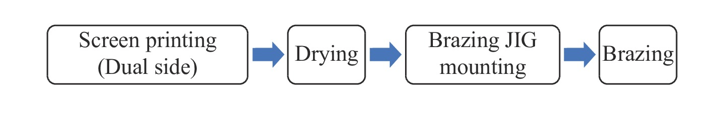
There are two main differences between DBC and AMB products: First, the copper and ceramics of DBC products are directly bonded, while the copper and ceramics of AMB products are brazed with active metal brazing materials, requiring additional screen printing processes. Before brazing, the active metal solder is evenly placed on the ceramic substrate; secondly, the copper of the DBC product is formed by one etching, and for the AMB product with an additional metal brazing layer, an additional etching process is required to remove the solder, usually hydrofluoric acid.
Taking AMB products as an example, the process flow of the ceramic copper substrate is shown in Figure 2, and the main processes and materials will be described in detail below.
1. Raw materials
The direct raw materials of ceramic copper substrate mainly include copper strip and ceramic substrate, as well as special active metal brazing filler metal (take AMB as an example).
Copper strip: Cu-OFE (copper> 99.99%, oxygen <0.0005%) is widely used in industry at present. It is supplied in strip form and should be pressed and cut into copper foil of the same size as the ceramic supplied before use. Since chemical pretreatment is required before bonding, there is no strict requirement on the storage life of the copper strip.
Active metal solder: It is a mixed paste material with certain adhesion. In order to prevent any change in its characteristics, it is usually stored at sub-zero temperature and should be thawed and mixed immediately before use.
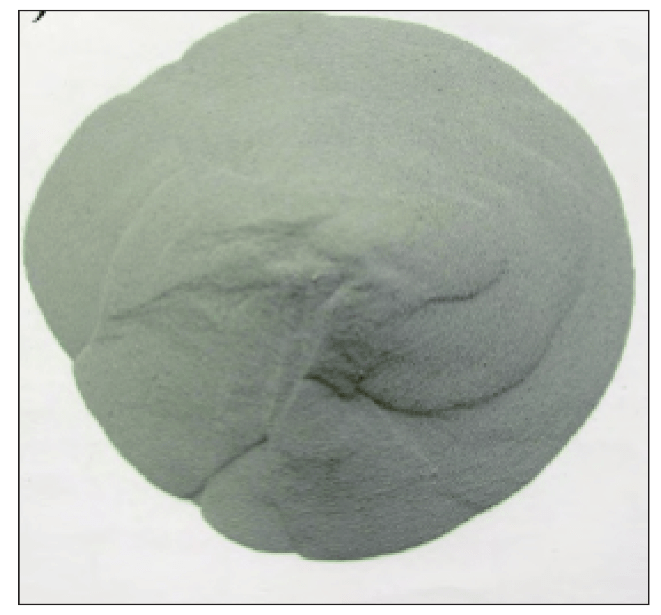
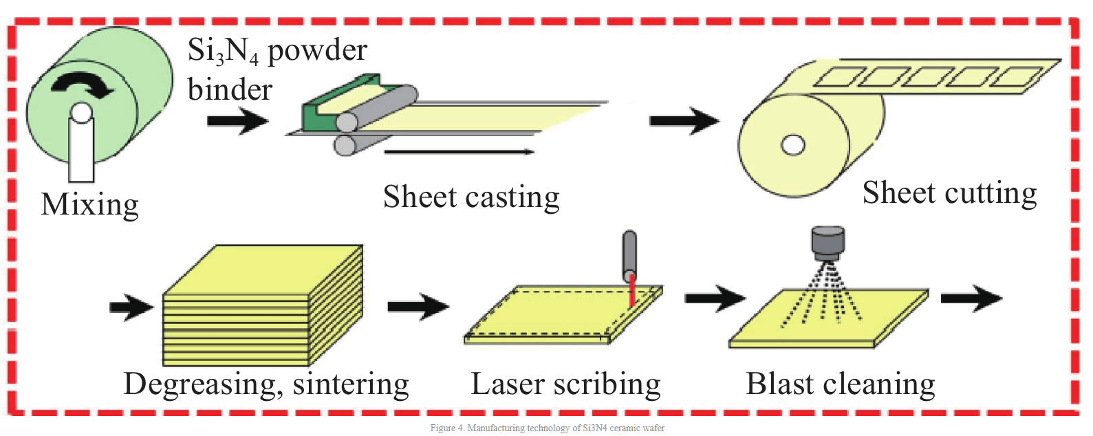
Ceramics: AMB and DBC use different ceramic materials. The ceramic materials used in DBC mainly include AI2O3 and AIN. Alumina is more mature than aluminum nitride in technology and has advantages in price. Therefore, 80% of DBC in the market uses alumina. The ceramic material used in AMB has a high thermal conductivity of Si3N4. Si3N4 is supplied in powder form. After a series of mixing, blending, printing, and molding, it can be processed into ceramic sheets required for AMB production. The powder type is shown in Figure 3, the flake type is shown in Figure 4, and the ceramic disc is shown in Figure 5.
Sheet type as shown in Figure 4
Ceramic disc as shown in Figure 5
2. Screen printing
Before screen printing, the active metal solder should be taken out of the sub-zero temperature environment and placed at room temperature for a period of time to ensure adhesion and printing performance. Before printing, the thawed active metal solder should be centrifuged and stirred to remove the bubbles in the solder, to ensure that the solvent and the active agent are fully mixed to prevent the lack of solder during printing. Specific as shown in Figure 6.
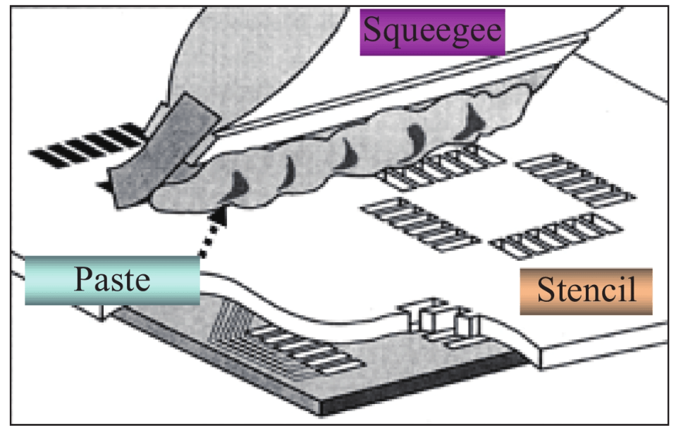
In order to ensure that there is enough solder on the surface of the ceramic sheet after printing, the ceramic sheet should be weighed and compared before and after printing. If the printing thickness is abnormal, the solder on the surface can be scrubbed with alcohol and printed.
3. Bonding/brazing
In the preparation of DBC, copper and metal are combined, and oxygen element is introduced between copper and ceramic substrate; then eutectic will be formed at 1065 ℃; after that, the ceramic substrate reacts with copper to generate CuAIO2 or Cu(AIO2), thus realizing the eutectic combination of copper and ceramic. The process principle is shown in FIG. 7.
The surface treated copper and ceramics will be taken and placed in the loading place of the vacuum furnace, and then put into the furnace cavity for bonding. The bonding process is the core of the entire DBC process and is the bottleneck that affects the yield (some domestic suppliers can only achieve 90% yield). Defects that affect yield are bubbles between the copper and the ceramic.
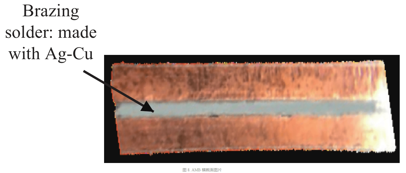
In the preparation of AMB, the active metal solder is used to combine copper and ceramic substrates, and the solder containing Ti/Ag/Cu and other elements chemically reacts with the ceramic to generate a reaction layer that can be wetted by the liquid solder, thus realizing the welding of metal on the surface of the workpiece without metallized ceramic. The process principle is shown in FIG. 8.
According to the cross-section shown in Figure 9, the solder is located between copper and ceramic, and its main element is Ag-Cu.
AMB substrate preparation technology is the development of DBC technology, the use of active metal solder to reduce the bonding temperature, thereby reducing the thermal stress of the ceramic substrate. Since the bonding of the AMB substrate is realized by using the chemical bond generated by the chemical reaction between the active metal solder and the ceramic, and the Si3N4 and AI2O3 used in the AMB have higher thermal conductivity and are used in the DBC, the AMB substrate can achieve better heat dissipation and insulation performance and higher reliability, so it can be used to carry high-power chips, mainly for electric vehicle power modules. DBC substrates are commonly used in small and medium power consumer electronics such as refrigerators and air conditioners.
目前,活性焊料的制备是制备AMB基板的关键技术。活性金属焊料可分为高温焊料(活性金属包括Ti、V和Mo,焊接温度为1000-1250℃)、中温焊料(活性金属包括Ag-Cu-Ti,载在 700-800 °C的保护气体或真空中进行焊接)和低温焊料(活性金属包括 Ce、Ga和Re,在200-300 °C的焊接温度下)。中高温活性焊料成分简单、操作方便、机械强度高,已广泛应用于金属-陶瓷结合。
Bubbles are also a critical defect of the AMB brazing process. Therefore, ultrasonic scanning is introduced after the bonding/brazing process to detect bubbles under the copper generated during the bonding/brazing process. Since hidden air bubbles will affect the overall heat dissipation of the semiconductor module, resulting in reliability risks when defective products are delivered to the semiconductor factory, the semiconductor factory will conduct reliability tests when verifying the ceramic copper substrate, including SAM (ultrasonic scanning) thermal shock 3000 times After the test, it checks whether there is delamination between copper and ceramic.
4. Lamination-etching
The etched pattern of the ceramic-copper substrate is formed by a lamination etching process, as shown in FIG. 10.
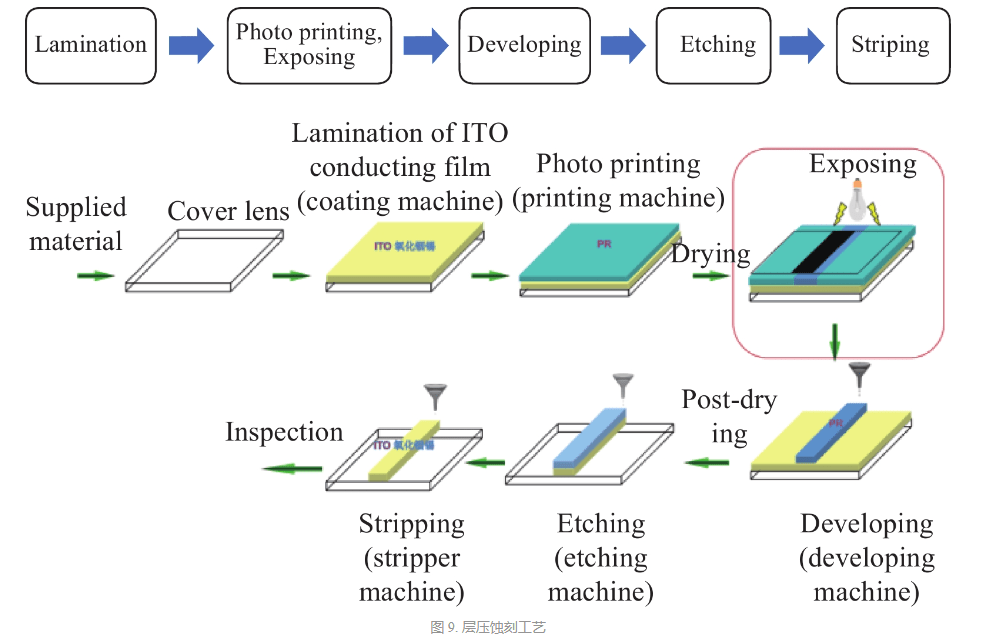
Bonding: A layer of ITO conductive film (Indium Tin Oxide) is plated on the entire mother card for conduction;
Photo printing: A photoresist material is plated on the surface of the mother card with ITO and baked. Due to the high sensitivity of photoresist materials, yellow light is required during the process;
曝光:紫外光穿透掩膜板照射到待曝光产品的光刻胶表面。紫外光可以穿透掩模版的透明部分撞击光刻胶引起光刻胶反应,但不能穿透掩模版的不透明黑色部分引起反应。通过这种方式,可以将掩模版上的图案投影到母卡上的光刻胶涂层上,
Development: After exposure, the developer is sprayed on the surface of the product to dissolve and remove the reacted photoresist on the surface of the mother card. The part that is not exposed to ultraviolet rays and does not react will remain on the surface of the main card,
Etching: After treatment with a developer, the mother card with the pattern is immersed in an acid solution for etching. Portions of the copper on the surface of the mother card that are not covered by the photoresist are etched away, leaving portions protected by the photoresist to form an etching pattern. The solder under the copper is not corroded by the acid solution. The etching depth can be controlled by controlling the concentration of the acid solution and the immersion time of the mother card (the speed of the steel strip) during the manufacturing process.
Stripping: Spray the stripping solution on the surface of the mother card after etching. The stripping solution dissolves the photoresist remaining on the surface of the mother card to expose the unetched copper surface, thereby forming an etching pattern of the first layer.
For lamination-etch processes, etch depth is an important IPC monitoring item. This is typically measured and the CPK performance will be monitored after stripping.
5. Second lamination-etching
For DBC products, a single etch creates the final pattern. However, when the AMB substrate is prepared, due to an additional layer of solder, the lamination etching process needs to be repeated, but the type of etching solution needs to be adjusted accordingly, for example, hydrofluoric acid can be used to remove the solder display ceramic substrate, so that the lines on the AMB surface meet the electrical performance requirements.
6. Electroplating
According to the customer's subsequent application, different coating treatments can be carried out on the surface of the ceramic-copper substrate. The commonly used coatings in the industry include silver plating, gold plating, and nickel plating. The silver plating process is illustrated by way of example, as shown in FIG. 11.
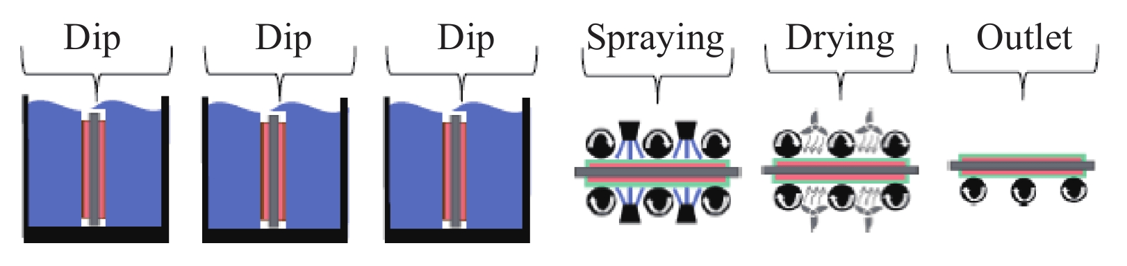
Before electroless plating, the copper on the surface of the ceramic copper substrate should be cleaned to remove foreign matter. The surface cleaned substrate should be acid treated again to remove the surface oxide. Thereafter, the substrate is etched and immersed in a plating solution to complete surface plating, and finally the surface of the substrate is cleaned and dried.
Electroplating thickness is an important IPC monitoring item in the electroplating process. The coating thickness can be measured by XRF(X-ray fluorescence spectrometer) for CPK monitoring. According to the current monitoring, the coating thickness of different places of the overall main card may vary greatly, which may cause large fluctuations in the coating thickness of the entire batch and affect the customer's application.
7, Laser cutting
After learning plating, the mother card is pre-cut along the sawing street by industrial laser to prepare for subsequent manual cutting. Since the copper is etched, the laser cutting mainly acts on the serrated road between the ceramic substrate and the cutting depth should be strictly controlled. Mainstream lasers in the industry include CO2 lasers (carbon dioxide lasers, as shown in FIG. 12) and USP lasers (ultrashort pulse lasers).
CO2激光器是一种气体分子激光器,工作物质为CO2,辅助气体包括氮气、氦气、氢气和氙气。利用CO2分子的振动和转动能级之间的跃迁,产生波长为10.6 μm的红外激光,具有更高的能量转换效率、更大的功率、更高的激光光束光学质量、更好的相干性和更高的工作效率。稳定性好,因此通常用于工业金属切削。
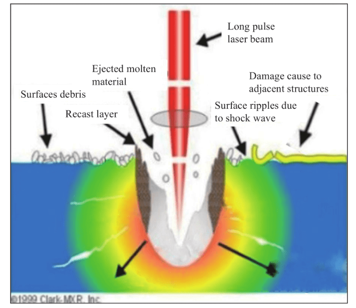
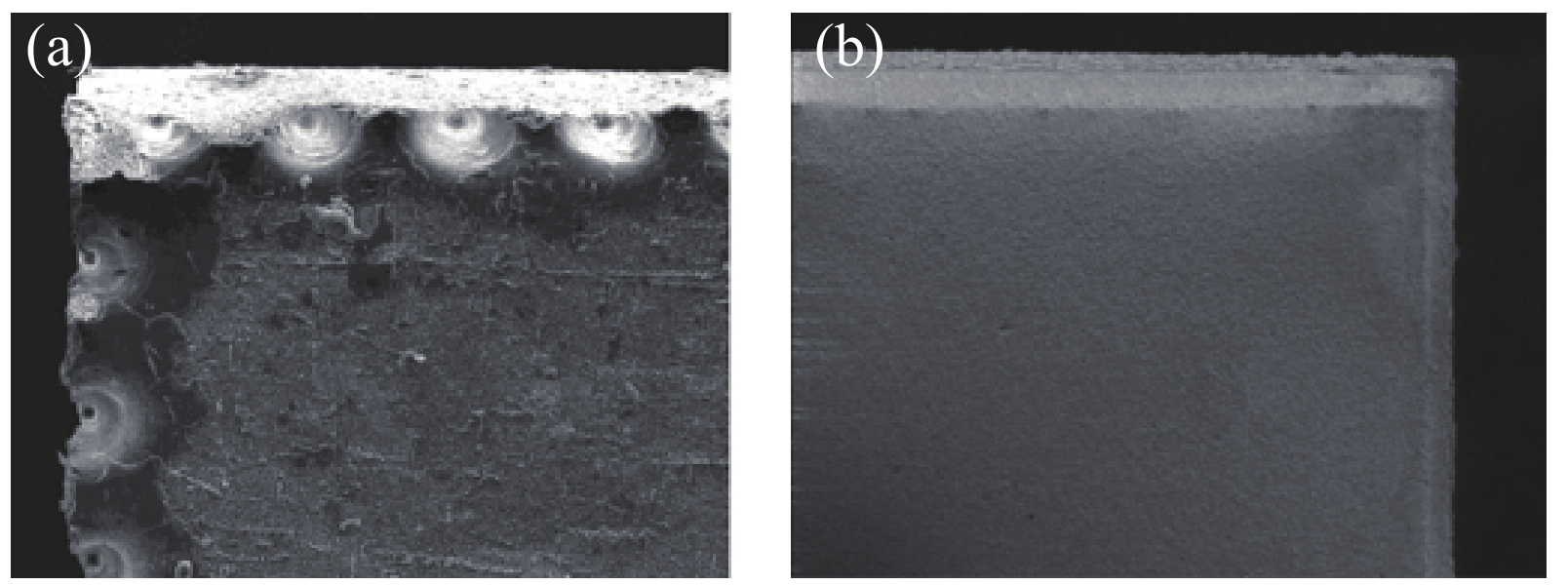
The cutting method of CO2 laser is single point impact, which will cause deep damage to the ceramic substrate. Figure 13 (a) surface morphology and (B) surface cross-section under single point impact SEM photos.
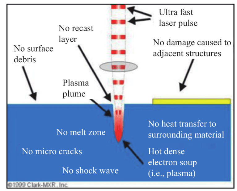
The so-called ultrashort pulses used in the USP laser (ultrashort pulse laser) are femtosecond laser pulses. The principle of generation of a typical Ti-doped sapphire crystal laser is shown in FIG. 14.
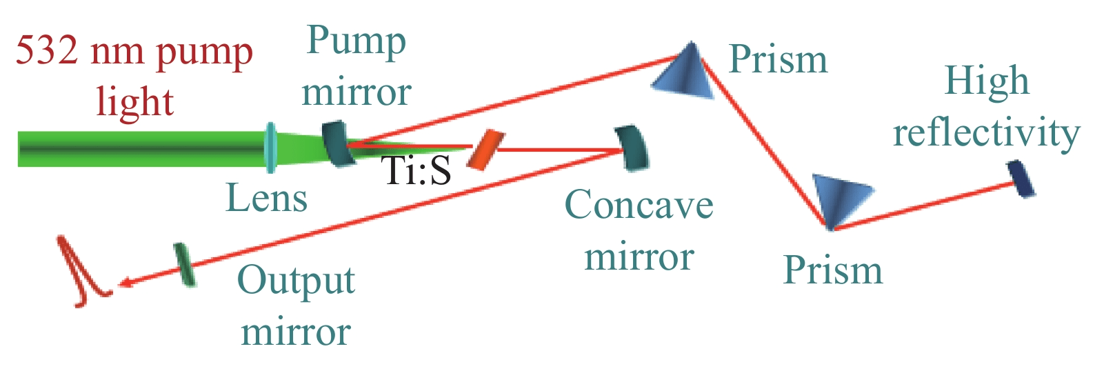
The ultra-short pulse laser has a nanometer wavelength and a peak power of 1015 watts, which can achieve energy concentration in a limited area and perform rapid processing. The USP laser is shown in Figure 15.
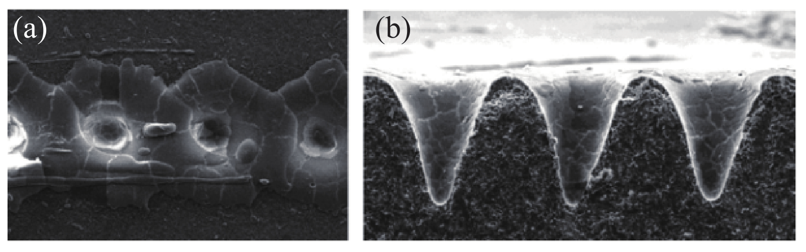
Compared with CO2 laser, the USP laser has less damage to the sawing lane on the ceramic, and the cutting surface forming effect is better. Due to its positive advantages, USP laser cutting is currently replacing CO2 lasers in some domestic factories and may be expanded to overseas suppliers. 16 for comparison (a) CO2 laser and (B) USP laser.
8. Monolithic
Since the mother card is not completely broken after laser cutting to form a single piece of ceramic substrate copper, it needs to be singulated. The strength shall be controlled during cutting to prevent edge chipping or cracking of the ceramic sheet. After slicing, the appearance of the microcontroller is fully inspected, and the corresponding defects are picked out and recorded. At present, the common defects are scratches, broken corners, corrosion holes, copper leakage and oxidation dirt.
Next Page
Related News
Celebrating the start of operation of Zhuhai Feizhida New Company
Shenzhen Feishida Machinery Equipment Co., Ltd. has opened a new company in Zhuhai Doumen Fushan Industrial Zone in order to develop the company's business and better serve customers. The company has one-stop service of designing, developing and selling PCB,FPC,HDI, ceramic board DBC,DPC ,AMB and other high-end horizontal lines. Production area of 30000 square meters. R & D workshop, engineering design workshop, production workshop. With more than 10 years of technical staff more than 200 people. Own research and development products have more than 100 kinds, recognized by many customers.
Shenzhen feishida mechanical equipment co., ltd. and Zhuhai feishida intelligent technology co., ltd. will participate in the 6th international ceramic circuit board IGBT exhibition from August 28 to 30, 2024, which will be held in Shenzhen baoan exhibition hall. At that time, we will display the latest equipment and the latest achievements. Welcome to guide.
Shenzhen Feishida's new heavy-duty full-automatic grinding machine is ceremoniously listed
Resin plug hole grinding machine
Zhuhai Feizhida Intelligent Technology Co., Ltd was established
On February 6, 2024, Zhuhai Feizhida Intelligent Technology Co., Ltd. established a new production base in Fushan Industrial Zone, Doumen District, Zhuhai, with a production workshop area of 300 million square meters and more than 200 new production technical employees. With a monthly production capacity of 800 meters, it mainly produces automation equipment: suitable for ceramic plates, carrier plates, HDI, and other high-grade intelligent equipment. For Zhuhai, Zhongshan, Jiangmen, Guangzhou, as well as domestic and foreign customers more convenient and efficient service.
Won the National High-tech Enterprise
Feishida has the factory area of Shenzhen and Zhuhai Feizhida Intelligent Technology Co., Ltd., covering an area of 30000 square meters, integrating R & D, production, sales and after-sales. It has more than 200 technical employees and a monthly production capacity of more than 800 meters.
With a monthly production capacity of 800 meters, it mainly produces automation equipment: suitable for ceramic plates, carrier plates, HDI, and other high-grade intelligent equipment. For Zhuhai, Zhongshan, Jiangmen, Guangzhou, as well as domestic and foreign customers more convenient and efficient service.


Shenzhen address: 201, Building 2, Xinweirun High tech Park, No. 3 Shajiang Road, Xitou Community, Songgang Street, Bao'an District, Shenzhen.
Zhuhai address: Building 10, No. 111 Qilu, Qianwu Town, Zhuhai


Sweep and add WeChat
Copyright @ Shenzhen Feishida Machinery Equipment Co., Ltd.


